
Platings > Gold-Tin Alloy Plating
Gold-Tin Alloy Plating
We offer a plating deposit as a lead-free solder for high-temperature connections, and as a solder for high-strength and high-reliability connections.
Both rack plating and barrel plating are available.
We can provide a thinner plating deposit than sheet material or ribbon material. And we can also form the deposit on the selected portion.
The eutectic and non-eutectic compositions of gold-tin alloys plating can be provided, too.
Our gold-tin alloy plating can be applied to the parts that require high-temperature connection or high-reliability connection.
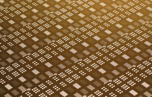
Precision Plating: Plating on Fine Patterns
Fine patterns on semiconductor wafers are the fundamental enabler of modern electronics, serving as the blueprint for billions of transistors and other integrated circuit elements. Shrinking these patterns is crucial for delivering high performance, low power consumption, and massive integration in today's devices.
At Mitsuya, we excel at this challenge, offering fine-pattern plating down to Φ25μm to help you realize your cutting-edge technology. We achieve this precision through proprietary process controls and decades of plating expertise, which ensures uniformity across the entire wafer.
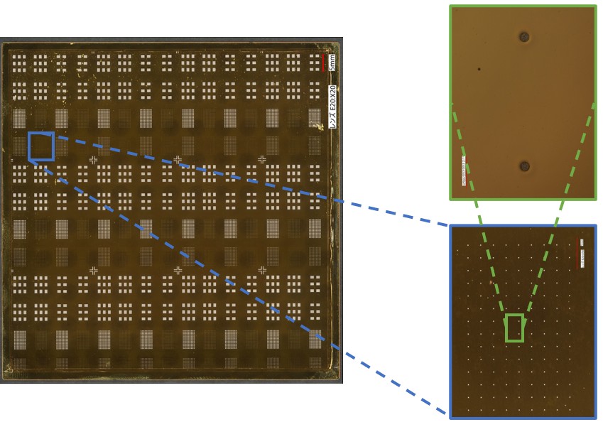
Fine Pattern on Wafer Φ25μm
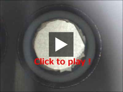
This movie shows the result of Mitsuya gold-tin plating deposit by DTA. You can see the melting vividly and dramatically at the eutectic point. (47sec.)
(* Any software to play MP4 movie file is required.)
Functional property
- Good Bondability
- Electrical Conductivity
- Low Contact Resistance
- High Temperature Solder
Industry employed
- Sensors
- Semi-conductor (IC)
- Optical Electronics
Solutions
Availability details
| mass production | yes |
|---|---|
| process type ※ | B,R |
| under plating | Cu,Ni,Pd-Ni,Ni-P |
| prototype | yes |
| experimental trial | yes |
| regular chemical stock | yes |
- ※
- B:barrelR:rackM:mesh basketH:reel to reel